CMOS Inverter Simulation with Synopsys Custom Compiler
This guide walks through creating, simulating, and analyzing a CMOS inverter schematic using Synopsys Custom Compiler and PrimeWave.
1. Library and Cell Setup
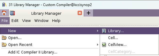
Create a new library:
- New → Library
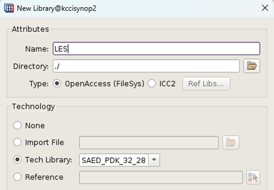
- Set attributes:
- Name: Library name
- Technology: Select tech library
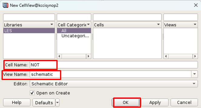
Create a new CellView:
- File → New → CellView
- Configure:
- Cell Name: Inverter
- View Name: schematic

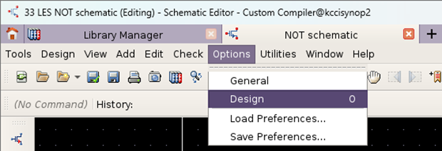
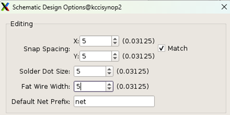
Design Settings:
Options → Design → Configure:
- Snap Spacing (X,Y): Grid spacing
- Solder Dot Size: Connection point size
- Fat Wire Width: Thick wire width
- Default Net Prefix: Signal prefix
2. Schematic Design
Add Components:
Use the Add tool (I=Instance, W=Wire, L=Label, P=Pin):
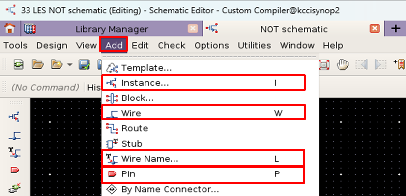
| I | W | L | P |
|---|---|---|---|
| Instance | Wire | Label | Pin |
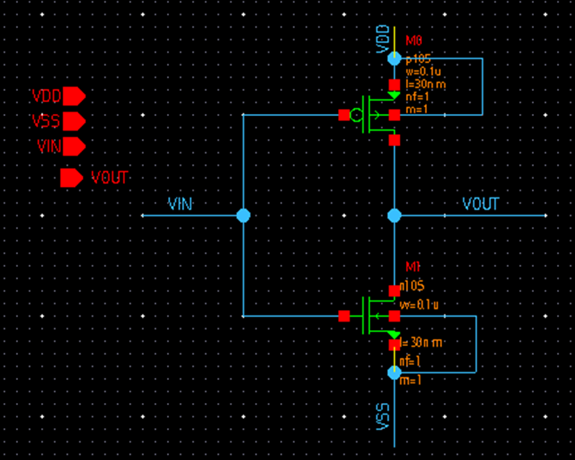
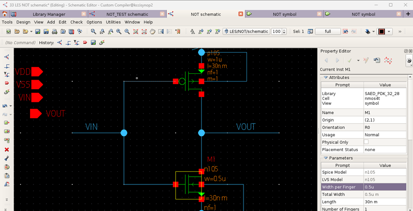
CMOS Inverter Schematic:
- Place PMOS and NMOS transistors
- Connect to VDD (top) and VSS (bottom)
- Add input (VIN) and output (VOUT) pins
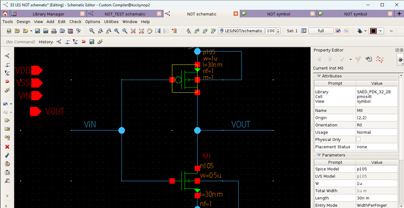
Component Properties:
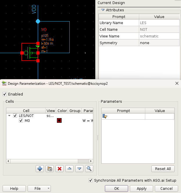
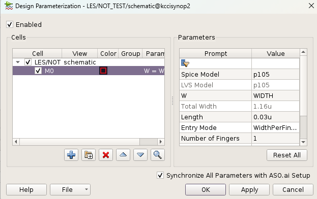
Select components → Press q → Configure:
- Transistor dimensions (W/L)
- Net connections
3. Symbol Creation
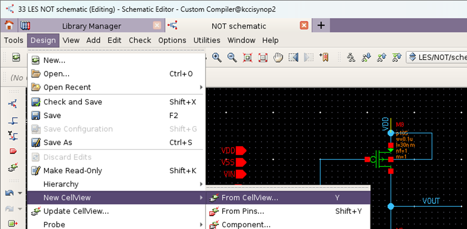
Generate Symbol:
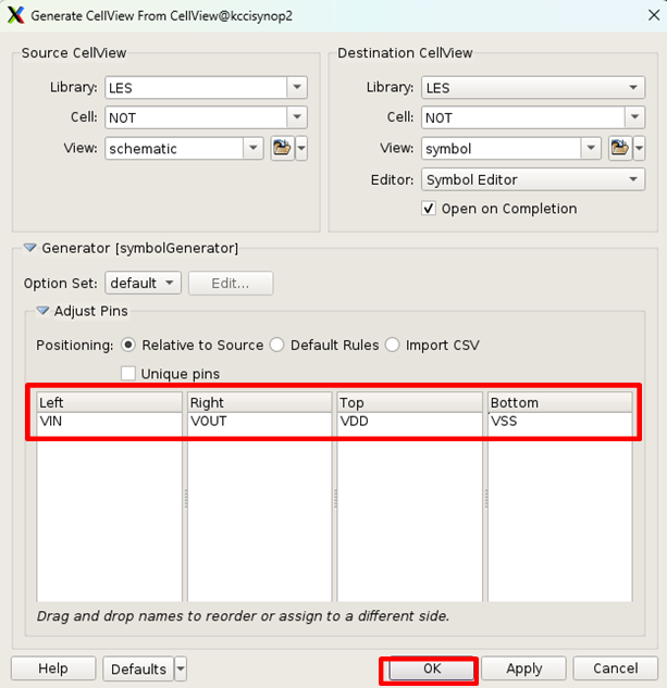
Pin Arrangement:
| Position | Pin Name |
|---|---|
| Left | VIN |
| Right | VOUT |
| Top | VDD |
| Bottom | VSS |
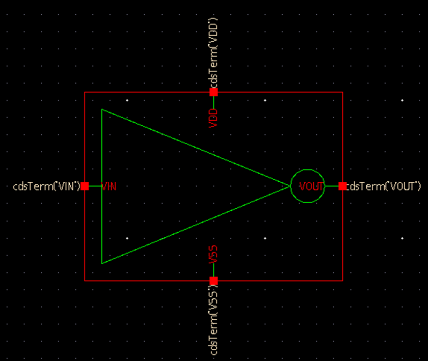
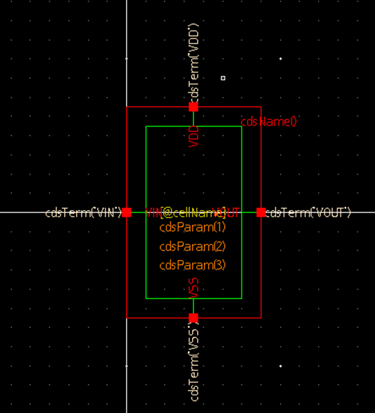
Final Inverter Symbol:
4. Test Schematic Setup
Create Testbench:

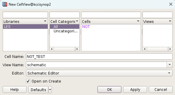
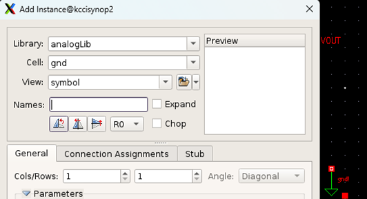
Add Components:
- Inverter symbol (Instance)
- Ground (GND)
- Voltage source (VDC)

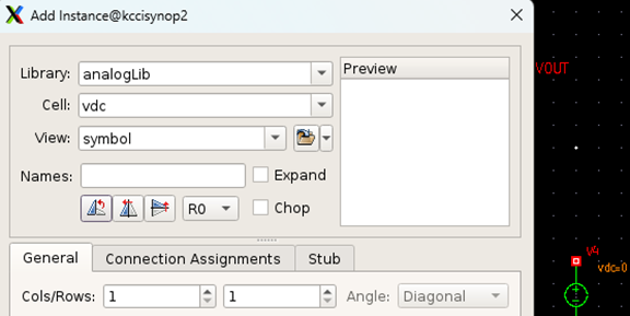
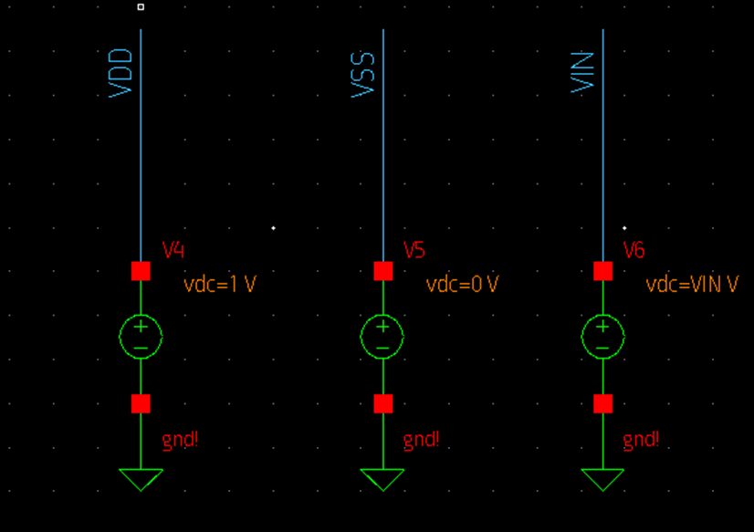
Configure Voltage Sources:
| Component | Property | Value |
|---|---|---|
| VDD | Voltage | 1.8V |
| VIN | Voltage | DC variable |
| VSS | Voltage | 0V |
5. Simulation with PrimeWave
Launch PrimeWave:

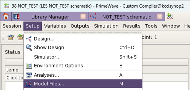
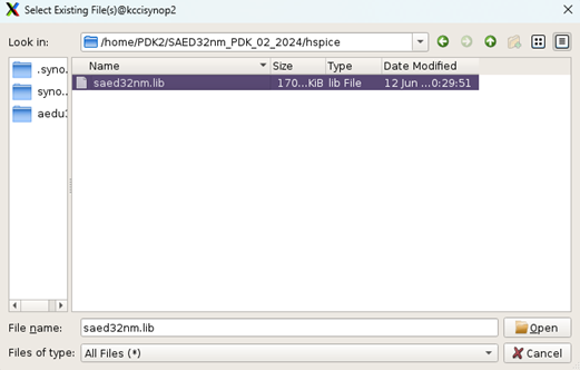
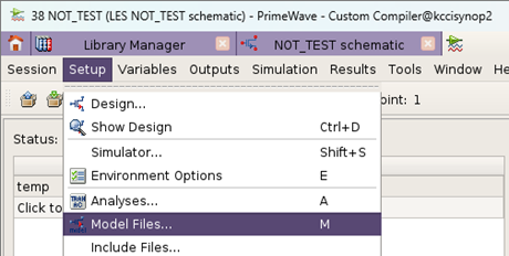
Set Model Files:

Configure Simulation:
- Model Section: Select (e.g., FF)
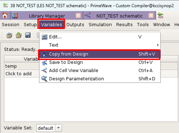
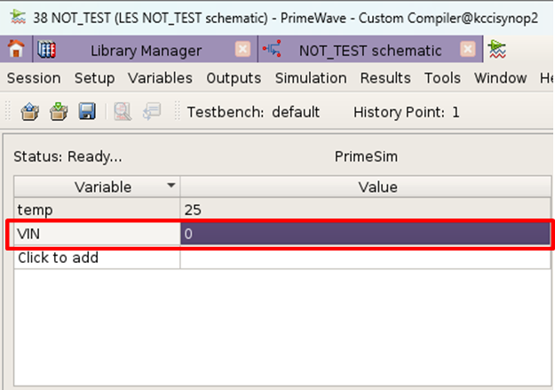
- Variables:
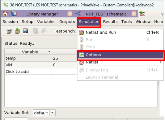
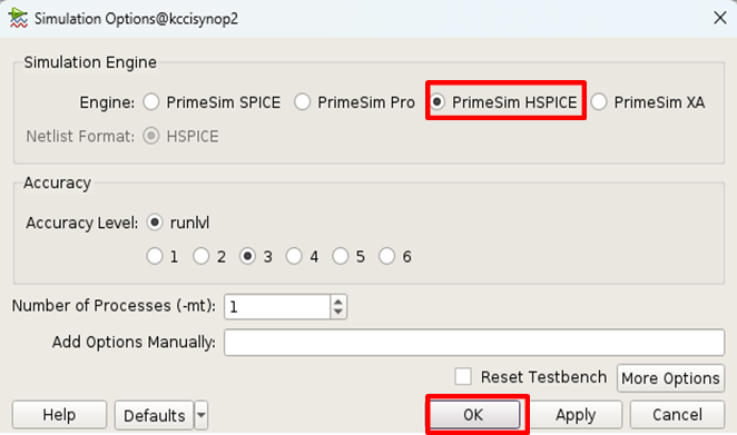
Copy from Design→ Set VIN=0 (설정하지 않으면 simulation이 안나올 수 있다) - Simulation Engine: PrimeSim HSPICE

Run Analysis:
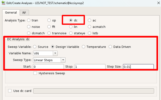
- Setup → Analyses
- Analysis Type: dc
- DC Analysis → Design Variable
- Variable Name, Sweep Type: VIN
- Start, Stop, Step Size: e.g., 0, 1.8, 0.01
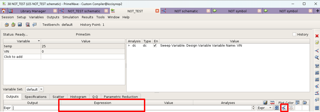
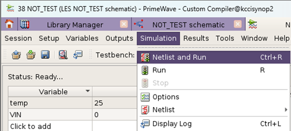
Run Simulation:
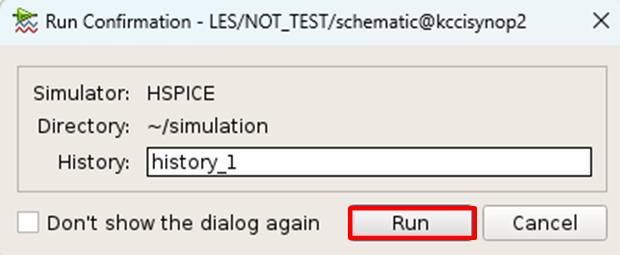
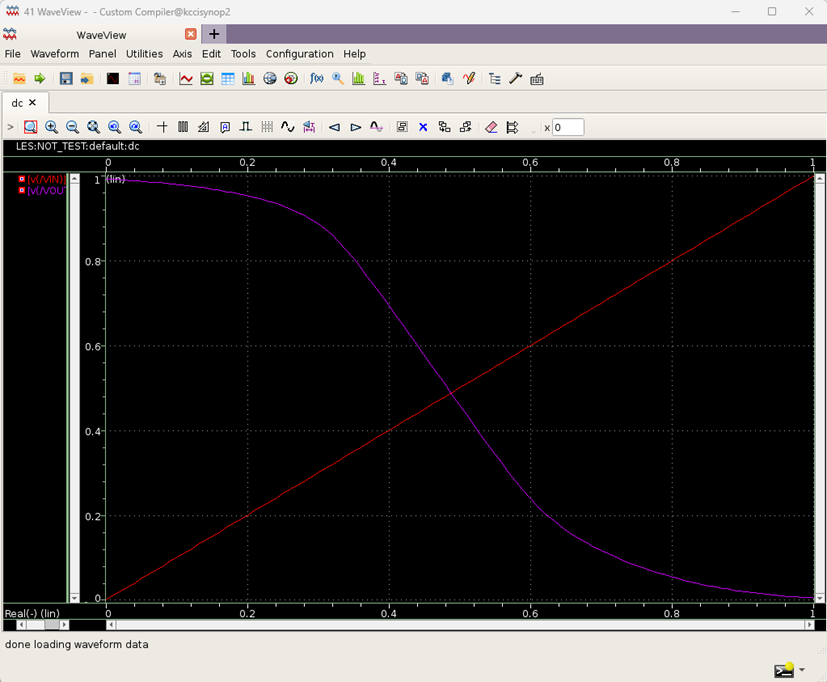
Results:
NOT WaveView
6. Troubleshooting
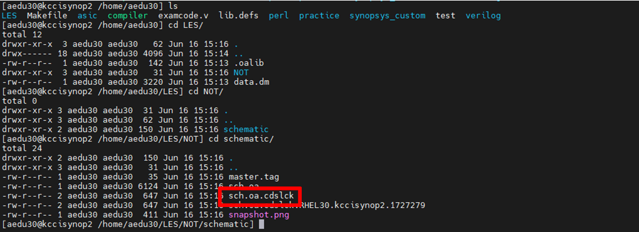
Schematic Lock Issue:
Delete lock file: *sch.oa.cdslck
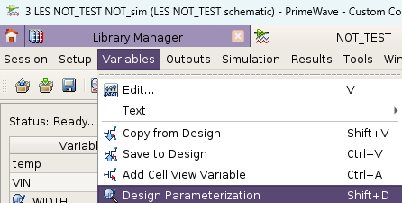
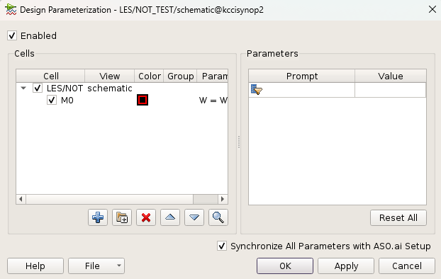
Advanced Configuration:
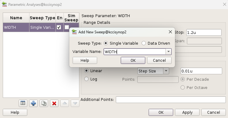
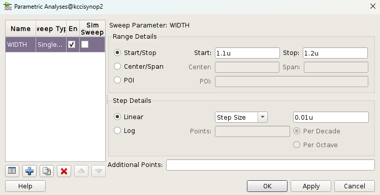
- Variable overrides
- Simulator options


Key Notes
- VIN Initialization: Must be set to 0V for DC sweep
- Model Selection: Use correct technology corner (e.g., FF)
- Port Connections: Verify VDD/VSS connections in test schematic
This structured guide ensures reproducible CMOS inverter simulation with clear visualization at each step.
